

Digital Logic Gates Explained: Truth Tables, Circuits and Classroom Projects
September 4, 2026
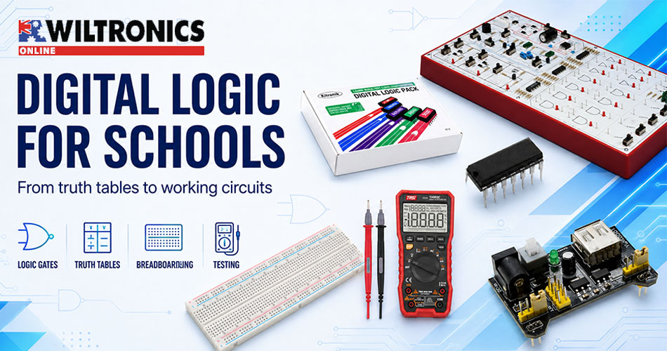
Digital Logic Gates Explained: Truth Tables, Circuits and Classroom Projects
Digital logic turns simple high and low electrical states into decisions. Every computer, calculator, digital clock, alarm controller and microcontroller depends on circuits that interpret binary information and produce predictable outputs.
Logic gates provide the building blocks. An AND gate can require two conditions before activating an output. An OR gate can respond to either condition. A NOT gate reverses a signal. By combining these simple functions, students can construct adders, alarms, memory circuits, counters and control systems.
This guide explains the major gate types, truth tables, Boolean expressions, logic families and practical circuit rules. It also provides a staged set of projects for school electronics, STEM classes and independent learning.
Classroom scope: Use regulated extra-low-voltage supplies and follow the voltage limits in every device datasheet. Do not connect breadboard logic circuits directly to mains power, automotive systems or other high-energy sources.
Digital logic at a glance
| Gate | Boolean expression | Output becomes 1 when… | Simple example |
|---|---|---|---|
| AND | Y = A · B | All inputs are 1 | Two safety switches both close |
| OR | Y = A + B | At least one input is 1 | Either alarm sensor activates |
| NOT | Y = ¬A | The input is 0 | A normally reversed indicator |
| NAND | Y = ¬(A · B) | Any input is 0 | Universal gate and control logic |
| NOR | Y = ¬(A + B) | Every input is 0 | “No condition active” detector |
| XOR | Y = A ⊕ B | Inputs differ | Two-way state comparison |
| XNOR | Y = ¬(A ⊕ B) | Inputs match | Equality detector |
The symbols 0 and 1 describe logic states, not universal voltages. A particular device family defines which input voltages count as LOW and HIGH.
Which logic gate do you need?
| Design requirement | Start with | Why |
|---|---|---|
| Activate only when every condition is true | AND | All inputs must be HIGH |
| Activate when any condition is true | OR | One or more HIGH inputs produce HIGH |
| Reverse a signal | NOT | The output becomes the opposite state |
| Build several functions from one gate type | NAND or NOR | Each can implement every Boolean function |
| Detect whether two inputs differ | XOR | The output becomes HIGH for unlike inputs |
| Detect whether two inputs match | XNOR | The output becomes HIGH for equal inputs |
| Add two binary bits | XOR and AND | XOR produces SUM; AND produces CARRY |
| Store a simple state | Cross-coupled NAND or NOR | Feedback retains one bit |
Classroom projects at a glance
Start with a single-gate truth-table test, then progress through an interlock, multi-input alarm, NAND-only conversion, half adder, one-bit latch and hardware-versus-software comparison. The detailed projects later in this guide include a learning focus for each stage.
What is a logic level?
A digital circuit divides a voltage range into recognised states:
- Logic 0 or LOW represents the lower voltage range.
- Logic 1 or HIGH represents the upper voltage range.
- A region between the guaranteed LOW and HIGH thresholds may produce an undefined result.
Datasheets specify VIL(max), the highest guaranteed LOW input, and VIH(min), the lowest guaranteed HIGH input. Output limits include VOL(max) and VOH(min) under stated loads. A source must meet the receiving input’s thresholds with adequate noise margin. “Both boards use 5V” does not prove compatibility, and a 3.3V HIGH may not satisfy every 5V input.
Texas Instruments’ logic-family selection guide compares CMOS and TTL-compatible thresholds across several low-voltage families. For classroom circuits, students should read the exact IC datasheet rather than assume every gate interprets voltage in the same way.
How to read a truth table
A truth table lists every possible input combination and the resulting output. A two-input gate has four combinations because each input can take two states:
| A | B | Possible state |
|---|---|---|
| 0 | 0 | Both LOW |
| 0 | 1 | A LOW, B HIGH |
| 1 | 0 | A HIGH, B LOW |
| 1 | 1 | Both HIGH |
With n independent binary inputs, a complete truth table contains 2ⁿ rows. Three inputs produce eight combinations; four inputs produce sixteen.
Truth tables connect a verbal rule, Boolean expression and circuit. For example:
“Turn on the warning light when the guard is open AND the machine-enable switch is on.”
Let A represent the guard-open signal, B represent machine enable, and Y represent the warning light. The requirement becomes Y = A · B.
AND gate: every condition must be true
An AND gate outputs HIGH only when every input is HIGH.
| A | B | Y = A · B |
|---|---|---|
| 0 | 0 | 0 |
| 0 | 1 | 0 |
| 1 | 0 | 0 |
| 1 | 1 | 1 |
AND logic suits interlocks and permission systems. A greenhouse fan might run only when temperature exceeds a threshold and an enable switch remains active. Implement this with a suitable gate, controller or switching circuit; do not wire arbitrary outputs together.
OR gate: any condition can activate the output
An OR gate outputs HIGH when one or more inputs are HIGH.
| A | B | Y = A + B |
|---|---|---|
| 0 | 0 | 0 |
| 0 | 1 | 1 |
| 1 | 0 | 1 |
| 1 | 1 | 1 |
An alarm can use OR logic when a door sensor, window sensor or emergency button should trigger the same indicator. In Boolean algebra, + represents OR rather than arithmetic addition.
NOT gate: reverse the input
A NOT gate, or inverter, uses one input and produces the opposite state.
| A | Y = ¬A |
|---|---|
| 0 | 1 |
| 1 | 0 |
NOT gates convert active-high signals to active-low behaviour and vice versa. A small circle, or inversion bubble, on a symbol indicates inversion; diagrams may also use an overbar, prime mark or ¬ symbol.
NAND gate: AND followed by NOT
A NAND gate produces the opposite of AND.
| A | B | Y = ¬(A · B) |
|---|---|---|
| 0 | 0 | 1 |
| 0 | 1 | 1 |
| 1 | 0 | 1 |
| 1 | 1 | 0 |
NAND acts as a universal gate because NAND combinations can reproduce every Boolean function. Joining a NAND gate’s inputs creates an inverter; additional stages can form AND, OR, XOR and storage circuits. Challenge students to recreate another gate and verify its full truth table.
NOR gate: OR followed by NOT
A NOR gate outputs HIGH only when every input is LOW.
| A | B | Y = ¬(A + B) |
|---|---|---|
| 0 | 0 | 1 |
| 0 | 1 | 0 |
| 1 | 0 | 0 |
| 1 | 1 | 0 |
NOR also functions as a universal gate. Cross-coupled NOR gates can form a set-reset latch that stores one bit.
XOR gate: detect a difference
An exclusive-OR gate outputs HIGH when its two inputs differ.
| A | B | Y = A ⊕ B |
|---|---|---|
| 0 | 0 | 0 |
| 0 | 1 | 1 |
| 1 | 0 | 1 |
| 1 | 1 | 0 |
XOR supports binary addition, parity and comparison. A half adder uses XOR for SUM and AND for CARRY. “One or the other, but not both” describes a two-input XOR; for devices with more inputs, follow the manufacturer’s truth table.
XNOR gate: detect a match
XNOR reverses XOR, so its output goes HIGH when the inputs match.
| A | B | Y = ¬(A ⊕ B) |
|---|---|---|
| 0 | 0 | 1 |
| 0 | 1 | 0 |
| 1 | 0 | 0 |
| 1 | 1 | 1 |
This equality function compares bits, confirms matching switch positions and contributes to multi-bit comparators.
Active-high and active-low signals
An active-high input performs its function when HIGH; an active-low input performs it when LOW. Schematics identify active-low signals with an inversion bubble, overbar, slash or suffix such as /RESET or RESET_N. Ask students to describe a circuit in two ways:
- the electrical state at each pin
- the meaning of the asserted function
This separates electrical level from labels such as “pressed”, “open” or “enabled”.
Boolean algebra: simplify before building
Boolean algebra describes logical relationships symbolically. Several identities help students reduce a circuit:
| Identity | Meaning |
|---|---|
| A · 1 = A | AND with TRUE changes nothing |
| A · 0 = 0 | AND with FALSE always gives FALSE |
| A + 0 = A | OR with FALSE changes nothing |
| A + 1 = 1 | OR with TRUE always gives TRUE |
| A + A = A | Repeating an OR input adds nothing |
| A · A = A | Repeating an AND input adds nothing |
| A + ¬A = 1 | A state or its inverse always covers all cases |
| A · ¬A = 0 | A state and its inverse cannot both be true |
De Morgan’s laws connect AND, OR and inversion:
- ¬(A · B) = ¬A + ¬B
- ¬(A + B) = ¬A · ¬B
These laws explain how NAND and NOR reproduce other functions. Students can prove each identity with matching truth tables before wiring it.
Combinational and sequential logic
Combinational logic produces outputs from present inputs; gates, multiplexers, decoders, comparators and adders fit this group. Sequential logic also uses stored state, allowing latches, flip-flops, registers and counters to remember earlier events.
This distinction creates a natural teaching progression:
- Test one gate.
- Combine gates into a decision circuit.
- Build a half adder.
- Create a latch that remembers a button press.
- Introduce clock pulses and counting.
Half adders and full adders
A half adder adds two one-bit numbers:
| A | B | SUM (XOR) | CARRY (AND) |
|---|---|---|---|
| 0 | 0 | 0 | 0 |
| 0 | 1 | 1 | 0 |
| 1 | 0 | 1 | 0 |
| 1 | 1 | 0 | 1 |
The final row shows 1 + 1 = 10₂: SUM becomes 0 and CARRY becomes 1. A full adder also accepts carry-in, so designers can chain stages into multi-bit adders.
Latches: storing one bit
Two cross-coupled NOR or NAND gates can form a set-reset latch. One input sets the output, another resets it, and feedback retains the state. NAND and NOR versions use different active levels, and some input combinations create prohibited or indeterminate conditions. Students should follow a verified circuit and record every transition. The activity introduces feedback, memory and state transitions before flip-flops, registers and counters.
CMOS versus TTL and TTL-compatible CMOS
The part number identifies more than the function. Logic families use different supplies, thresholds, drive capabilities and timing. Classic TTL commonly operates from nominal 5V. CMOS can provide lower static power and different voltage ranges. 74HC uses CMOS input thresholds; 74HCT combines CMOS construction with TTL-compatible thresholds at its specified supply.
Do not mix families solely because the part numbers contain the same final digits. A 74HC00 and 74HCT00 both contain four two-input NAND gates, but their guaranteed input thresholds differ. Nexperia’s 74HC00 and 74HCT00 documentation provides a useful example.
Before connecting devices, compare:
- recommended supply-voltage range
- VIH and VIL input limits
- VOH and VOL output limits
- source and sink current
- maximum input rise and fall times
- propagation delay
- package and pinout
- operating temperature
Why floating inputs cause trouble
A disconnected CMOS input does not reliably select 0 or 1. Its high impedance allows noise, leakage and nearby electric fields to move the voltage through the switching region. The output may change unpredictably, and a slowly changing input can increase current inside the device.
Give every input a defined state. A switch input usually needs a pull-up or pull-down resistor so the gate sees a valid level when the switch opens. Tie unused inputs to an appropriate logic level according to the datasheet; do not leave them floating.
Texas Instruments discusses this issue in its standard-logic datasheet guide and low-voltage logic design guide. Use the value and connection recommended for the device and application rather than adopting one resistor value for every family.
Switch bounce and slow edges
Mechanical switch contacts rarely change state once and cleanly. They can bounce between open and closed for a short time. A simple LED may hide this activity, but a counter or latch can interpret one press as several events.
Debouncing methods include:
- an RC network followed by a suitable Schmitt-trigger input
- a dedicated debounce circuit
- an SR latch with an appropriate changeover switch
- software timing when a microcontroller reads the switch
Do not feed a slow analogue ramp into an ordinary digital input unless its datasheet permits that transition rate. A Schmitt-trigger input adds hysteresis and produces cleaner switching between defined thresholds.
Propagation delay: logic takes time
Propagation delay measures the time between an input transition and the corresponding output change. Delays accumulate through gate chains, and unequal paths can briefly produce a glitch. Timing diagrams reveal this effect even when classroom instruments cannot resolve the shortest pulses. Supply voltage, temperature, capacitance and load all influence timing.
Output loading and LED indicators
A logic output can source or sink only limited current while maintaining a valid voltage. Never connect an LED without a current-limiting resistor, and do not assume a gate can directly power a relay, motor, lamp or high-current LED.
For an LED indicator, calculate the resistor from:
R = (Vsupply − VLED) ÷ ILED
Then check the logic output’s voltage and current specifications. A conservative indicator current often gives ample visibility with less output loading, but the actual choice depends on the LED, gate family and circuit.
Use a suitable transistor, MOSFET or driver stage when the load exceeds the logic output’s rating. Add flyback protection across an inductive DC load where the switching design requires it.
Decoupling and breadboard layout
Digital switching creates brief current demands and electrical noise. Place a suitable ceramic decoupling capacitor close to each IC’s supply pins, following the manufacturer’s recommendation. Connect the circuit ground consistently and keep signal paths orderly.
On a solderless breadboard:
- identify which holes share internal contacts
- check whether long power rails contain breaks
- connect every IC supply pin correctly
- orient DIP packages across the centre channel
- add decoupling near each IC
- use consistent wire colours
- keep inputs defined
- switch off power before moving components
- inspect for off-by-one-row wiring errors
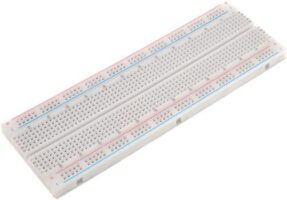
The reusable 830-point solderless breadboard provides a practical base for these circuits. Add the 140-piece breadboard jumper kit or 65 flexible male-pin jumper wires to keep signal paths organised. The broader breadboards and prototyping range supports different project sizes.
Choosing a practical learning platform
| Pathway | Best for | Main advantage | Planning consideration |
|---|---|---|---|
| IEC Electronics Digital Trainer | Repeatable school laboratory lessons | Built-in components and guided experiments | Higher initial investment per station |
| Kitronik Digital Logic Pack | Linking gates with BBC micro | Connects hardware decisions with code | Requires the compatible Inventor’s Kit and micro pathway |
| Loose ICs and breadboard | Open-ended electronics construction | Develops pinout reading and fault-finding | Requires careful component selection and more setup |
IEC Electronics Digital Trainer
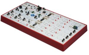
The IEC Electronics Digital Trainer provides a structured teaching panel for foundational electronics and digital logic. Its built-in components support work with rectification, filtering, regulation, oscillators, transistors, basic gates and counting circuits.
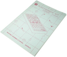
This platform suits schools that want repeatable experiments without rebuilding every circuit. The IEC Digital Trainer Experiment Manual provides guided activities, while a replacement cover and work tray supports long-term classroom use.
Choose the IEC trainer when consistency, durability and repeatable laboratory setup matter most.
Kitronik Digital Logic Pack and micro
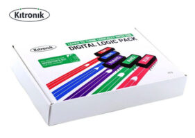
The Digital Logic Pack for the Kitronik Inventor’s Kit contains AND, OR, XOR, NAND and NOT-gate ICs, two MOSFETs, jumper wires and circuit-identification stickers. Students can use the gates with the micro to compare hardware logic with programmed Boolean decisions.

The pack extends the Kitronik Inventor’s Kit for BBC micro, which supplies a broader pathway into breadboarding and physical computing.
Choose the Kitronik pathway when students should compare physical gates with Boolean expressions in code.
Loose ICs and breadboards
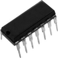
Loose ICs demand more preparation but develop strong pinout-reading, construction and troubleshooting skills. A quad two-input AND-gate IC provides one starting point. Browse the integrated-circuit range and check every device datasheet.
Choose breadboarding when open-ended construction and fault-finding form core learning outcomes.
Seven classroom logic projects
| Project | Student task | Learning focus |
|---|---|---|
| Verify one gate | Test every switch combination and compare the LED output with a truth table | Binary states and systematic evidence |
| Two-condition interlock | Activate an output only when two model conditions become true | Translating a design rule into AND logic |
| Multi-sensor alarm | Use OR logic so either input activates an indicator or suitably driven sounder | Multiple inputs controlling one response |
| NAND-only conversion | Recreate NOT, AND and OR using only NAND gates | Universal gates and De Morgan’s laws |
| Half adder | Display XOR SUM and AND CARRY outputs on separate LEDs | Binary arithmetic and parallel processing |
| One-bit memory | Build a guided SR latch and record set, reset and prohibited states | Feedback, state and memory |
| Hardware versus code | Reproduce a physical gate’s truth table in a micro program | Connecting Boolean logic, hardware and software |
A five-lesson teaching sequence
| Lesson | Concept | Practical outcome |
|---|---|---|
| 1 | Binary states and truth tables | Students test AND, OR and NOT gates |
| 2 | NAND, NOR and Boolean identities | Students construct one gate from another |
| 3 | XOR and arithmetic | Students build a half adder |
| 4 | Feedback and memory | Students investigate an SR latch |
| 5 | Design and evaluation | Students solve an interlock, alarm or comparison brief |
Assess students on more than whether the final LED illuminates. Ask them to predict outputs, document pin connections, record all truth-table rows, explain faults and justify their chosen gate arrangement.
Downloadable worksheet opportunity
Add a one-page companion worksheet with blank two- and three-input truth tables, gate-symbol identification, Boolean-expression prompts and space for predictions versus measured results. This can attract educator searches, support classroom use and provide a clear downloadable resource linked from the article.
Troubleshooting digital logic circuits
| Symptom | Likely cause | What to check |
|---|---|---|
| Output changes when a hand approaches | Floating input | Add the correct pull-up, pull-down or defined connection |
| LED never turns on | Reversed LED, wrong pinout, no supply or incorrect logic | Check polarity, resistor, IC orientation, VCC and ground |
| LED always stays on | Misread active-low signal, floating input or wiring error | Compare circuit with the truth table and pin diagram |
| One button press creates several counts | Contact bounce | Add an appropriate debounce method |
| Different IC families do not communicate | Incompatible thresholds or supplies | Compare VIH, VIL, VOH, VOL and voltage ratings |
| IC becomes warm | Incorrect supply, output contention or excessive load | Disconnect power immediately and inspect wiring |
| Circuit works until another LED connects | Output overloaded or supply unstable | Calculate load current and improve decoupling |
| Results change at higher speed | Propagation delay, long wiring or poor signal integrity | Shorten paths and inspect timing requirements |
A disciplined fault-finding order saves time:
- Switch off power and inspect the layout.
- Confirm the IC part number, orientation and pinout.
- Verify the supply voltage at the IC pins.
- Check ground continuity.
- Confirm that every input has a defined level.
- Test one gate and one truth-table row at a time.
- Measure the output without overloading it.
- Reconnect later stages only after the first stage works.
Equipment for a classroom logic station
A practical group station may include:
- an IEC Electronics Digital Trainer or 830-point breadboard
- compatible logic-gate ICs, such as the Digital Logic Pack or 4011 quad NAND-gate IC
- a regulated extra-low-voltage source, such as the 3.3V/5V breadboard power-supply module
- momentary pushbuttons or suitable switches
- a 5mm LED assortment and suitable metal-film resistors
- breadboard jumper wires, flexible jumper leads or compatible trainer leads
- 0.1µF monolithic ceramic capacitors for decoupling, or a ceramic capacitor assortment
- an economy digital multimeter
- suitable tweezers or forceps for careful IC handling
- printed truth tables and pin diagrams, supported by the IEC Electronics Digital Trainer Experiment Manual
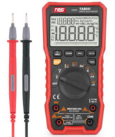
The Wiltronics multimeter range includes options for checking supply voltage and continuity. Teachers should demonstrate correct lead sockets, function selection and parallel voltage measurement before students test circuits.
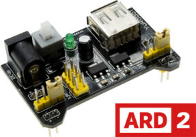
The 3.3V/5V breadboard power module can power compatible projects when students observe its input, output and current limits.
For a fully structured laboratory system, start with the IEC Electronics Digital Trainer. With physical computing, combine the Kitronik Digital Logic Pack with the compatible Inventor’s Kit and micro. For open-ended construction, use breadboards and datasheet-verified logic ICs.
Frequently asked questions
What are the seven basic logic gates?
They are AND, OR, NOT, NAND, NOR, XOR and XNOR. AND, OR and NOT provide the foundational operations; NAND and NOR invert those results and can each implement any other Boolean function; XOR and XNOR compare whether inputs differ or match.
What voltage represents logic 1?
No single voltage applies to every device. The IC family, supply voltage and datasheet define the guaranteed HIGH and LOW input ranges. Check VIH and VIL before connecting different families or voltage domains.
Why should I never leave a logic input floating?
A floating input can collect noise and drift through an undefined voltage region, causing unpredictable switching and increased current. Connect unused and switch-controlled inputs to defined states according to the datasheet.
Why do NAND and NOR count as universal gates?
Designers can combine only NAND gates—or only NOR gates—to reproduce NOT, AND, OR and every other Boolean function. This makes either gate type sufficient for constructing a complete combinational logic system.
What is the difference between XOR and OR?
OR outputs HIGH when either or both inputs are HIGH. A two-input XOR outputs HIGH only when the inputs differ, so it returns LOW when both inputs are HIGH.
What is the difference between combinational and sequential logic?
Combinational outputs depend only on current inputs. Sequential logic also uses stored state, so earlier inputs can affect the present output.
Can a logic gate power a motor or relay directly?
Usually not. Logic outputs have limited current capability. Use a properly designed transistor, MOSFET or driver stage and the required protection components for the load.
Do 74HC and 74HCT mean the same thing?
No. They may provide the same logic function and pin arrangement, but 74HC uses CMOS input thresholds while 74HCT provides TTL-compatible thresholds under its specified operating conditions. Always compare datasheets.
From simple gates to complete digital systems
Logic gates give students a visible way to understand how electronic systems make decisions. Truth tables establish the rules, Boolean algebra simplifies them, and practical circuits reveal the importance of voltage thresholds, defined inputs, timing and output loading.
Begin with AND, OR and NOT. Progress to NAND, NOR and XOR, then combine gates into adders, latches and design challenges. The same principles extend into microcontrollers, programmable logic, computers and industrial control systems.
Explore the IEC Electronics Digital Trainer, Kitronik Digital Logic Pack, integrated circuits and breadboarding equipment available from Wiltronics.
© Electrotech Brands Pty Ltd 2026
Write a Comment
You must be logged in to post a comment.